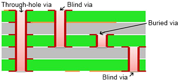
Blind And Buried Vias Fabrication

14 Layers Blind And Buried Vias Pcb Circuit Board Suppliers Pcb Circuit Board Circuit Board Printed Circuit Board

Blind Buried Vias Pcb Prototype The Easy Way Pcbway

Ipc 2226 Standard For Hdi Pcb Design Hdi Board Manufacturer Pcb Design Conductive Materials Printed Circuit Board

Ipc 2226 Standard For Hdi Pcb Design Hdi Board Manufacturer Pcb Design Circuit Board Printed Circuit Board

Ipc 2226 Standard For Hdi Pcb Design Hdi Board Manufacturer Pcb Design Printed Circuit Board Conductive Materials

Ipc 2226 Standard For Hdi Pcb Design Hdi Board Manufacturer Pcb Design Printed Circuit Board Circuit Board

10 000 served customers in 80 countries.
Blind and buried vias fabrication.

Ipc 2226 Standard For Hdi Pcb Design Hdi Board Manufacturer Pcb Design Printed Circuit Board Circuit Board
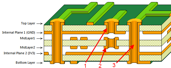
Blind And Buried Via E3 General Electronics
Pcb Via Plating Through Hole Blind Via Hole And Buried Via Hole Latest Open Tech From Seeed Studio

Laser Drilling Pcb Printed Circuit Board Drill Circuit Board

6 Layer Pcb With Blind Via And Buried Vias Manufacture And Making Pcba For Your Products Printed Circuit Board Circuit Board Circuit

Ipc 2226 Standard For Hdi Pcb Design Hdi Board Manufacturer Pcb Design Circuit Board Printed Circuit Board

Ipc 2226 Standard For Hdi Pcb Design Hdi Board Manufacturer Pcb Design Printed Circuit Board Circuit Board
Design Limitations Of Blind And Buried Vias Bittele

Rigao Electronics Provides High Quality Pcb Fabrication For Multi Layer Pcb Board Buried Blind Holes Pc Printed Circuit Boards Circuit Board Printed Circuit

Ipc 2226 Standard For Hdi Pcb Design Hdi Board Manufacturer Pcb Design Printed Circuit Board Circuit Board

Ipc 2226 Standard For Hdi Pcb Design Hdi Board Manufacturer Pcb Design Printed Circuit Board Circuit Board

32 Layer Printed Circuit Boards Printed Circuit Boards Circuit Board Circuit

Something We Loved From Instagram Chemical Free Pcb Fab Assembly Pcb Pabmanufacture Pcbdesign Pcbproto Pcb Design Circuit Board Chemical Free
Blind And Buried Via Pcbs Bittele

Flexible Printed Circuit Board Stiffeners Printed Circuit Board Circuit Board Circuit

Ipc 2226 Standard For Hdi Pcb Design Hdi Board Manufacturer Pcb Design Circuit Board Printed Circuit Board

Ipc 2226 Standard For Hdi Pcb Design Hdi Board Manufacturer Pcb Design Printed Circuit Board Conductive Materials

Pin By Pcb Board Assembly On Https Pcbboardassembly Com Process Control Printed Circuit Boards Printed Circuit Board

Ipc 2226 Standard For Hdi Pcb Design Hdi Board Manufacturer Pcb Design Printed Circuit Board Circuit Board

Ipc 2226 Standard For Hdi Pcb Design Hdi Board Manufacturer Pcb Design Circuit Board Printed Circuit Board
Failure Analysis Of Blind Via For Empty Cave In Pcb Filling Copper Plating

Super Thin 0 15mm Thickness Fr4 Pcb Board Prototype With Images Pcb Board Printed Circuit Boards Printed Circuit Board

All About Prepreg Pp In Printed Circuit Board Published By Fuchuangke On Edocr Printed Circuit Board Circuit Board Printed Circuit

Base Material Fr4 1 6mm Taiyo Psr4000 Solder Mask Taiyo Psr4000 Taimura Dsr2200 Probimer 77 Ma Matt Green Techn Printed Circuit Board Pcb Board Blue Mask

Ipc 2226 Standard For Hdi Pcb Design Hdi Board Manufacturer Pcb Design Circuit Board Printed Circuit Board

Pcb Board Printedcircuit Boards Pcb Boards Pcb Manufacturer Supplier Circuit Boards Single Doubed Sided Circuit Board Pcb Board Solutions

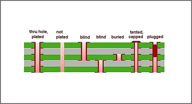
Pcb Vias Everything You Need To Know Blind Vias And Buried Vias

Pcb Global Prototype Quick Turn High Technology Printed Circuit Boards

Ipc 2226 Standard For Hdi Pcb Design Hdi Board Manufacturer Pcb Design Circuit Board Printed Circuit Board

Modern Electronics Major Events In The History Of Printed Circuit Boards Electronic Parts Printed Circuit Boards Circuit Board
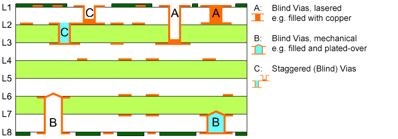
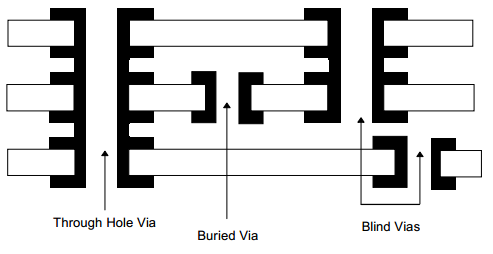
Blind Vias Buried Vias Multi Circuit Boards

Authentic Pcb Dna Unmatched Quality Pcblayout Fore More Details Url Https Www Pc Circuit Board Printed Circuit Board

How To Reduce Pcb Cost With Blind Buried Vias

Basics About Pick And Place Pcb Design With Images Pcb Design Design Basic

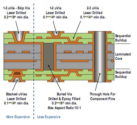
Reduce Your Pcb Costs With Blind Vias Buried Vias Microvias Blog Jaapson Blog And Resource Center
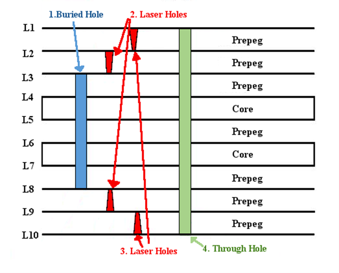
Pth Drilling In Hdi Circuits Hardwarebee
Pcb Via Size Complete Information It S Here Ourpcb

Bga Reballing Services Bga Diy Window Things To Come

Blind And Buried Via Pcb

Difference Between Ipc A 610 And The Ipc J Std 001 Courses Std Good To Know Certified Trainer
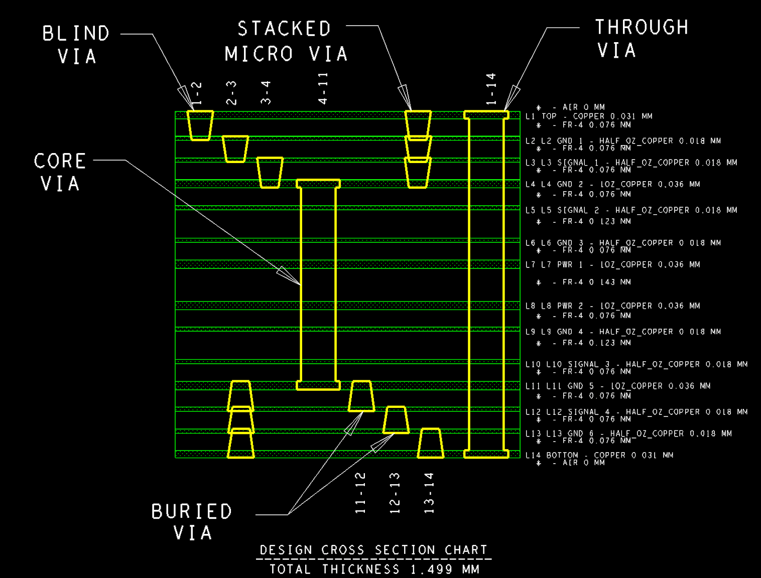
Confessions Of A Pcb Designer Anatomy Of A Via By John Burkhert Jr Supplyframe Medium

Carbon Oil Rigid Fr4 Multilayer Pcb Multi Layering Oils Carbon

Modern Electronics Major Events In The History Of Printed Circuit Boards Electronic Parts Printed Circuit Boards Circuit Board

Home Printed Circuit Board Circuit Board Printed Circuit
Source : pinterest.com
